- 您现在的位置:买卖IC网 > Sheet目录2005 > LTC1859IG#TRPBF (Linear Technology)IC A/D CONV 8CH 16BIT 28-SSOP
LTC1857/LTC1858/LTC1859
15
185789fa
0
1
2
3
4
5
6
7
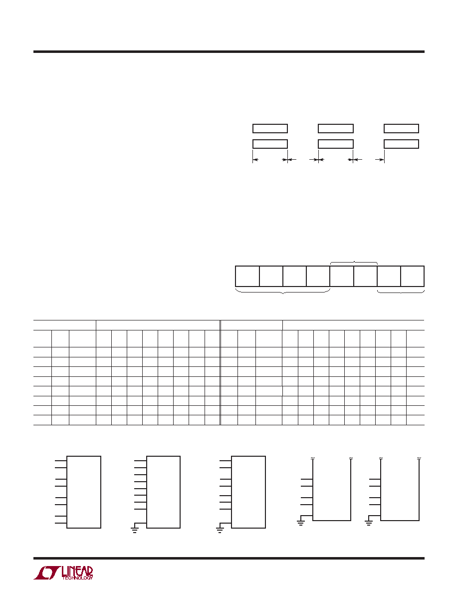
CHANNEL
COM (
–)
8 Single-Ended
+
0,1
CHANNEL
4 Differential
2,3
4,5
6,7
+ (–)
+
+ (–)
– (+)
4
5
6
7
CHANNEL
COM (
–)
Combinations of
Differential and Single-Ended
+
0,1
2,3
–
COM (UNUSED)
Changing the
MUX Assignment “On the Fly”
COM (
–)
4,5
6,7
4,5
1ST CONVERSION
2ND CONVERSION
+
–
+
–
+
–
+
7
6
{
1859 F08
APPLICATIONS INFORMATION
three-state at this time. When the conversion is complete
(BUSY goes high), CONVST and RD go low to enable the
data output for the previous conversion.
SERIAL DATA INPUT (SDI) INTERFACE
The LTC1857/LTC1858/LTC1859 communicate with micro-
processors and other external circuitry via a synchronous,
full duplex, 3-wire serial interface (see Figure 7). The shift
clock (SCK) synchronizes the data transfer with each bit
being transmitted on the falling SCK edge and captured
on the rising SCK edge in both transmitting and receiving
systems. The data is transmitted and received simultane-
ously (full duplex).
An 8-bit input word is shifted into the SDI input which
congures the LTC1857/LTC1858/LTC1859 for the next
conversion. Simultaneously, the result of the previous
conversion is output on the SDO line. At the end of the
data exchange the requested conversion begins by ap-
plying a rising edge on CONVST. After tCONV, the conver-
sion is complete and the results will be available on the
next data transfer cycle. As shown below, the result of a
conversion is delayed by one conversion from the input
word requesting it.
SGL/
DIFF
SELECT
1
SELECT
0
UNI
GAIN
NAP
MUX ADDRESS
INPUT RANGE
POWER DOWN
SELECTION
1859 AI02
ODD
SIGN
SLEEP
SDI
SDO
SDO WORD 0
SDI WORD 1
DATA
TRANSFER
SDO WORD 2
SDI WORD 3
SDO WORD 1
SDI WORD 2
DATA
TRANSFER
tCONV
A/D
CONVERSION
tCONV
A/D
CONVERSION
1859 AI01
Figure 8. Examples of Multiplexer Options on the LTC1857/LTC1858/LTC1859
INPUT DATA WORD
The LTC1857/LTC1858/LTC1859 8-bit data word is clocked
into the SDI input on the rst eight rising SCK edges. Fur-
ther inputs on the SDI pin are then ignored until the next
conversion. The eight bits of the input word are dened
as follows:
Table 1. Multiplexer Channel Selection
MUX ADDRESS
DIFFERENTIAL CHANNEL SELECTION
MUX ADDRESS
SINGLE-ENDED CHANNEL SELECTION
SGL/
DIFF
ODD
SIGN
SELECT
1 0
01234567
SGL/
DIFF
ODD
SIGN
SELECT
1 0
01234567
COM
0
0 0
+
–
1
0
0 0
+
–
0
0 1
+
–
1
0
0 1
+
–
0
1 0
+
–
1
0
1 0
+
–
0
1 1
+
–
1
0
1 1
+
–
0
1
0 0
–
+
1
0 0
+
–
0
1
0 1
–
+
1
0 1
+
–
0
1
1 0
–
+
1
1 0
+
–
0
1
1 1
–
+
1
1 1
+
–
发布紧急采购,3分钟左右您将得到回复。
相关PDF资料
LTC1867AIGN#TRPBF
IC ADC 16BIT 8CH 200KSPS 16SSOP
LTC1867LCGN#PBF
IC ADC 16BIT 8CH 175KSPS 16SSOP
LTC2142IUP-14#PBF
IC ADC DUAL 14BIT 65MSPS 64QFN
LTC2143CUP-14#PBF
IC ADC DUAL 14BIT 80 MSPS 64-QFN
LTC2153IUJ-14#PBF
IC ADC 14BIT DUAL 310MSPS 40QFN
LTC2158IUP-14#TRPBF
IC ADC DUAL 14BIT 310M 64-QFN
LTC2172IUKG-14#TRPBF
IC ADC 14BIT SER/PAR 65M 52-QFN
LTC2175IUKG-14#TRPBF
IC ADC 14BIT 125MSPS QUAD 52QFN
相关代理商/技术参数
LTC1860CMS8
功能描述:IC A/D CONV 1CH 12BIT 8-MSOP RoHS:否 类别:集成电路 (IC) >> 数据采集 - 模数转换器 系列:- 标准包装:2,500 系列:- 位数:16 采样率(每秒):15 数据接口:MICROWIRE?,串行,SPI? 转换器数目:1 功率耗散(最大):480µW 电压电源:单电源 工作温度:-40°C ~ 85°C 安装类型:表面贴装 封装/外壳:38-WFQFN 裸露焊盘 供应商设备封装:38-QFN(5x7) 包装:带卷 (TR) 输入数目和类型:16 个单端,双极;8 个差分,双极 配用:DC1011A-C-ND - BOARD DELTA SIGMA ADC LTC2494
LTC1860CMS8#PBF
功能描述:IC A/D CONV 1CH 12BIT 8-MSOP RoHS:是 类别:集成电路 (IC) >> 数据采集 - 模数转换器 系列:- 标准包装:1 系列:microPOWER™ 位数:8 采样率(每秒):1M 数据接口:串行,SPI? 转换器数目:1 功率耗散(最大):- 电压电源:模拟和数字 工作温度:-40°C ~ 125°C 安装类型:表面贴装 封装/外壳:24-VFQFN 裸露焊盘 供应商设备封装:24-VQFN 裸露焊盘(4x4) 包装:Digi-Reel® 输入数目和类型:8 个单端,单极 产品目录页面:892 (CN2011-ZH PDF) 其它名称:296-25851-6
LTC1860CMS8#TR
功能描述:IC A/D CONV 1CH 12BIT 8-MSOP RoHS:否 类别:集成电路 (IC) >> 数据采集 - 模数转换器 系列:- 标准包装:2,500 系列:- 位数:16 采样率(每秒):15 数据接口:MICROWIRE?,串行,SPI? 转换器数目:1 功率耗散(最大):480µW 电压电源:单电源 工作温度:-40°C ~ 85°C 安装类型:表面贴装 封装/外壳:38-WFQFN 裸露焊盘 供应商设备封装:38-QFN(5x7) 包装:带卷 (TR) 输入数目和类型:16 个单端,双极;8 个差分,双极 配用:DC1011A-C-ND - BOARD DELTA SIGMA ADC LTC2494
LTC1860CMS8#TRPBF
功能描述:IC A/D CONV 1CH 12BIT 8-MSOP RoHS:是 类别:集成电路 (IC) >> 数据采集 - 模数转换器 系列:- 标准包装:2,500 系列:- 位数:16 采样率(每秒):15 数据接口:MICROWIRE?,串行,SPI? 转换器数目:1 功率耗散(最大):480µW 电压电源:单电源 工作温度:-40°C ~ 85°C 安装类型:表面贴装 封装/外壳:38-WFQFN 裸露焊盘 供应商设备封装:38-QFN(5x7) 包装:带卷 (TR) 输入数目和类型:16 个单端,双极;8 个差分,双极 配用:DC1011A-C-ND - BOARD DELTA SIGMA ADC LTC2494
LTC1860CS8
功能描述:IC A/D CONV 1CH 12BIT 8-SOIC RoHS:否 类别:集成电路 (IC) >> 数据采集 - 模数转换器 系列:- 标准包装:2,500 系列:- 位数:16 采样率(每秒):15 数据接口:MICROWIRE?,串行,SPI? 转换器数目:1 功率耗散(最大):480µW 电压电源:单电源 工作温度:-40°C ~ 85°C 安装类型:表面贴装 封装/外壳:38-WFQFN 裸露焊盘 供应商设备封装:38-QFN(5x7) 包装:带卷 (TR) 输入数目和类型:16 个单端,双极;8 个差分,双极 配用:DC1011A-C-ND - BOARD DELTA SIGMA ADC LTC2494
LTC1860CS8#PBF
功能描述:IC A/D CONV 1CH 12BIT 8-SOIC RoHS:是 类别:集成电路 (IC) >> 数据采集 - 模数转换器 系列:- 标准包装:2,500 系列:- 位数:16 采样率(每秒):15 数据接口:MICROWIRE?,串行,SPI? 转换器数目:1 功率耗散(最大):480µW 电压电源:单电源 工作温度:-40°C ~ 85°C 安装类型:表面贴装 封装/外壳:38-WFQFN 裸露焊盘 供应商设备封装:38-QFN(5x7) 包装:带卷 (TR) 输入数目和类型:16 个单端,双极;8 个差分,双极 配用:DC1011A-C-ND - BOARD DELTA SIGMA ADC LTC2494
LTC1860CS8#PBF
制造商:Linear Technology 功能描述:IC ADC 12BIT 250KSPS SOIC-8 制造商:Linear Technology 功能描述:IC, ADC, 12BIT, 250KSPS, SOIC-8
LTC1860CS8#TR
功能描述:IC A/D CONV 1CH 12BIT 8-SOIC RoHS:否 类别:集成电路 (IC) >> 数据采集 - 模数转换器 系列:- 标准包装:2,500 系列:- 位数:16 采样率(每秒):15 数据接口:MICROWIRE?,串行,SPI? 转换器数目:1 功率耗散(最大):480µW 电压电源:单电源 工作温度:-40°C ~ 85°C 安装类型:表面贴装 封装/外壳:38-WFQFN 裸露焊盘 供应商设备封装:38-QFN(5x7) 包装:带卷 (TR) 输入数目和类型:16 个单端,双极;8 个差分,双极 配用:DC1011A-C-ND - BOARD DELTA SIGMA ADC LTC2494